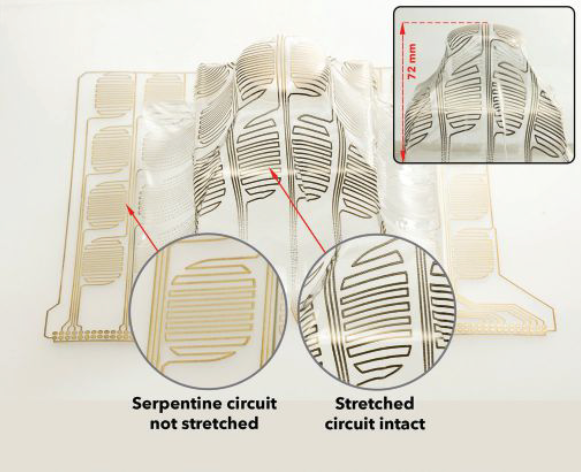
Thermoforming as a design tool in printed-electronics applications
To date, the benefits of two-dimensional (2D) printed electronics have been widely realized when the printed flat components can be integrated into the target device without many design constraints. However, it often can be challenging to fit the printed 2D surfaces fully conformally onto complex surfaces of a 3D device, germane particularly to wearable electronics. Whereas 3D printing rapidly is developing into a viable technology to obtain such complex structures and interconnects, it is an inherently slow process and, thus, is not scalable enough for industry needs. In contrast, if a 2D print design, having been accomplished by a normal R2R-printing/coating process, later is modified by thermalmolding into a quasi-3D object, it will be a highly efficient and reliable process. Currently, this firm is developing such a thermoforming process by using conductive silver ink onto a polycarbonate surface and checking the integrity of the circuits of the thermoformed objects.
Click the link below to download the full article.
This post is for members only
SubscribeAlready have an account? Log in